|
How To Restore An Original, 50-Year-Old Apollo Guidance Computer With A Little Assist From Terasic DE0-Nano Board
Written by Steven Leibson | Senior Content Manager at Intel®
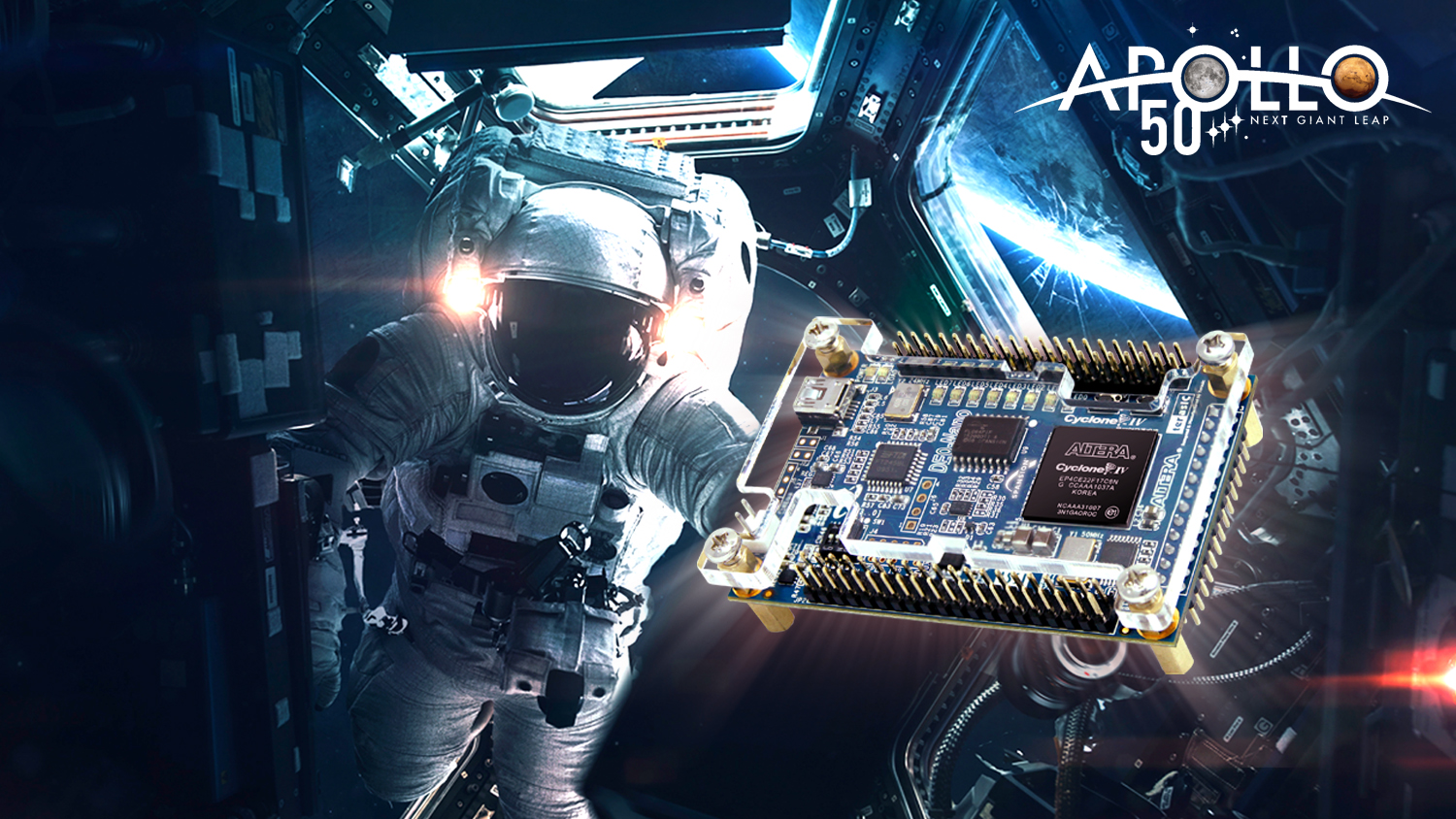
July 20, 2019 marks the 50th anniversary of the Apollo 11 Moon landing, the first time that a human being stepped upon a celestial body other than the Earth. Many, many commemorative activities are planned and many more have already taken place to celebrate this anniversary, but perhaps one of the coolest, from an engineering perspective, is the revival of a Block II Apollo Guidance Computer (AGC) by an intrepid team in the San Francisco Bay area. The restoration team includes Marc Verdiell (Atherton, CA), Ken Shirriff (Redwood City, CA), Carl Claunch (Los Altos, CA), and Mike Stewart (South San Francisco). A 26-episode (so far) YouTube playlist chronicles the team’s months’-long AGC restoration adventure. The AGC in question is owned privately by Jimmie Loocke, who worked as a thermal vacuum test technician at NASA during the Apollo space program. Loocke acquired the AGC as part of a 2-ton lot of surplus NASA equipment that he purchased in the 1970s. (This is quite a story all by itself.)
The AGC was instrumental in navigating to the Moon and back and landing all of the astronauts on the Moon for Apollo 11, 12, 13, 14, 15, 16, and 17. An AGC in the Apollo Command Module (CM) navigated from Earth to the Moon and back again. Another AGC in the Lunar Module (LM) helped to land on the Moon and then to take off from the Moon and to rendezvous with the CM in orbit around the Moon.
The AGC is a historic computer for many, many reasons. One of these resaons is the AGC’s connection to Moore’s Law. Nearly everyone in the electronics industry, especially in semiconductors, is familiar with Moore’s Law and with the graph that Gordon Moore drew in 1965 that led him to formulate the concept that became known as Moore’s Law. Moore used five specific semiconductor devices to plot that graph and, until recently, no one could recall the devices represented by those five dots. However, David Laws, who is the Semiconductor Curator at the Computer History Museum in Mountain View, put two early semiconductor artifacts together to reverse engineer the Moore’s Law plot. (See “Moore’s Law and the Seven Devices ,"on EEJournal.com for further details. In addition, for a more detailed version of the IC story behind the AGC’s design, see David Laws’ article titled “Silicon Chips Take Man to the Moon" on the Computer History Museum’s Web site.)
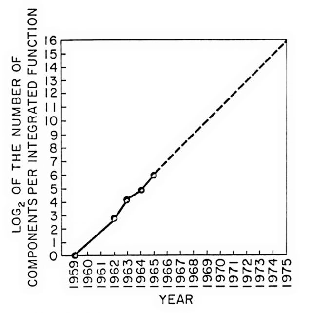 |
| The graph that led Gordon Moore to formulate what became known as Moore’s Law plotted five existing semiconductor devices. The second dot represents the IC that was used to design the original Block I Apollo Guidance Computer. |
The Moore’s Law story intersects the AGC story at one specific point on the original Moore’s Law curve. It’s the second dot, which represents a Fairchild Semiconductor μLogic Type G RTL IC. This device reaches so far back into the past that the terms "μLogic" and "Type G" are now virtually unknown and the term "RTL," which originally meant “resistor-transistor logic," now means something entirely different. In the FPGA world and the world of digital chip design, “RTL” stands for “register-transfer level.” Not the same thing at all.
The Fairchild Semiconductor μLogic Type G RTL IC was a 3-input NOR gate. That’s right, one gate per integrated circuit. That one gate per chip represented the high point in semiconductor manufacturing circa 1962.
Back then, the IC’s future was not at all certain. For example, an article that appeared in EDN magazine in 1960 noted:
“The weight and size of batteries and solar cells is the main problem in missile and space electronics – not the size of the electronics package…
"Whether standard modules are practical or not is still a point of controversy within the industry."
However, NASA placed severe restrictions on the AGC’s size and weight to meet the Apollo program’s overall design budgets. Consequently, when NASA selected MIT’s Instrumentation Lab to develop the AGC for the Apollo program, the computer’s designers knew that they would need to develop the AGC using the most revolutionary, lightweight, miniaturized electronics technology available at the time. The technology that qualified was the Type G IC.
On February 27, 1962, the MIT Instrumentation Lab ordered 100 Fairchild μLogic Type G ICs at the price of $43.50 each (in 1962 dollars!) for evaluation. Within a few months, the MIT Instrumentation Lab concluded that, yes, ICs were a very good thing to use for the Apollo Guidance Computer and used 4100 of them to implement all of the logic in the Block I AGC’s design. By 1965, the AGC program had purchased some 200,000 Type G logic chips at an average price of $20 to $30 each. The IC’s future had become very bright.
Fast forward to today. Jimmie Loocke’s Block II AGC had not been powered on for half a century. Its operational status was unknown.
Ultimately, many obstacles stood in the way of the team’s successful effort to get Loocke’s AGC operational in time for the 50th anniversary celebrations of the Apollo 11 Moon landing. The specific obstacles that are the basis for this blog were embedded in the AGC’s memory.
The AGC was designed with two types of memory: essentially RAM and ROM. However, semiconductor memory had not yet been invented so the AGC’s ROM was a magnetic rope memory and its RAM was magnetic core memory.
You may be familiar with core memory. It dominated computer memory from 1953 to 1971. Mainframe and minicomputers designed in the 1950s and 1960s all used core memory for RAM. Core memory stores ones and zeroes in thousands of ferrite rings that are hand woven into a wire grid. Hand-made core memory is expensive and, because it’s made by hand, not especially compact. Although many efforts were made to automate core memory fabrication, these efforts were largely unsuccessful. Then, in October, 1970, Intel introduced the first large semiconductor memory: the 1 kilobit 1103 DRAM. In just a couple of years, DRAM completely supplanted core memory because it was denser, faster, and less expensive. Core memory’s 20-year reign ended rather abruptly and the 1103 DRAM became Intel’s first big, game-changing hit.
Although related to core memory, rope memory was far less common and was used mainly for aerospace applications. Computer programs are actually woven into rope memory by hand, so each rope memory assembly was unique. To change programs, you needed to physically swap out the rope-memory module. Weaving programs by hand is an expensive, labor-intensive affair, so semiconductor ROMs quickly replaced rope memory as soon as they became available.
Jimmie Loocke acquired his AGC without any rope-memory modules and his AGC’s core memory ultimately turned out to be non-operational (although it was later repaired). However, as it happens, these memory-related challenges didn’t stop the AGC restoration effort. Mike Stewart, one of the AGC restoration team members, had previously replicated the AGC hardware using the original AGC schematics. Despite several design challenges, he managed to replicate the entire AGC including the function of its core and rope memories in an FPGA. More specifically, he created an AGC hardware emulation inside of a Terasic DE0-Nano FPGA development board, which is based on a Cyclone® IV FPGA, using the Intel® Quartus® Prime Software Suite to replicate the AGC’s design.
Terasic DE0-Nano Development Board
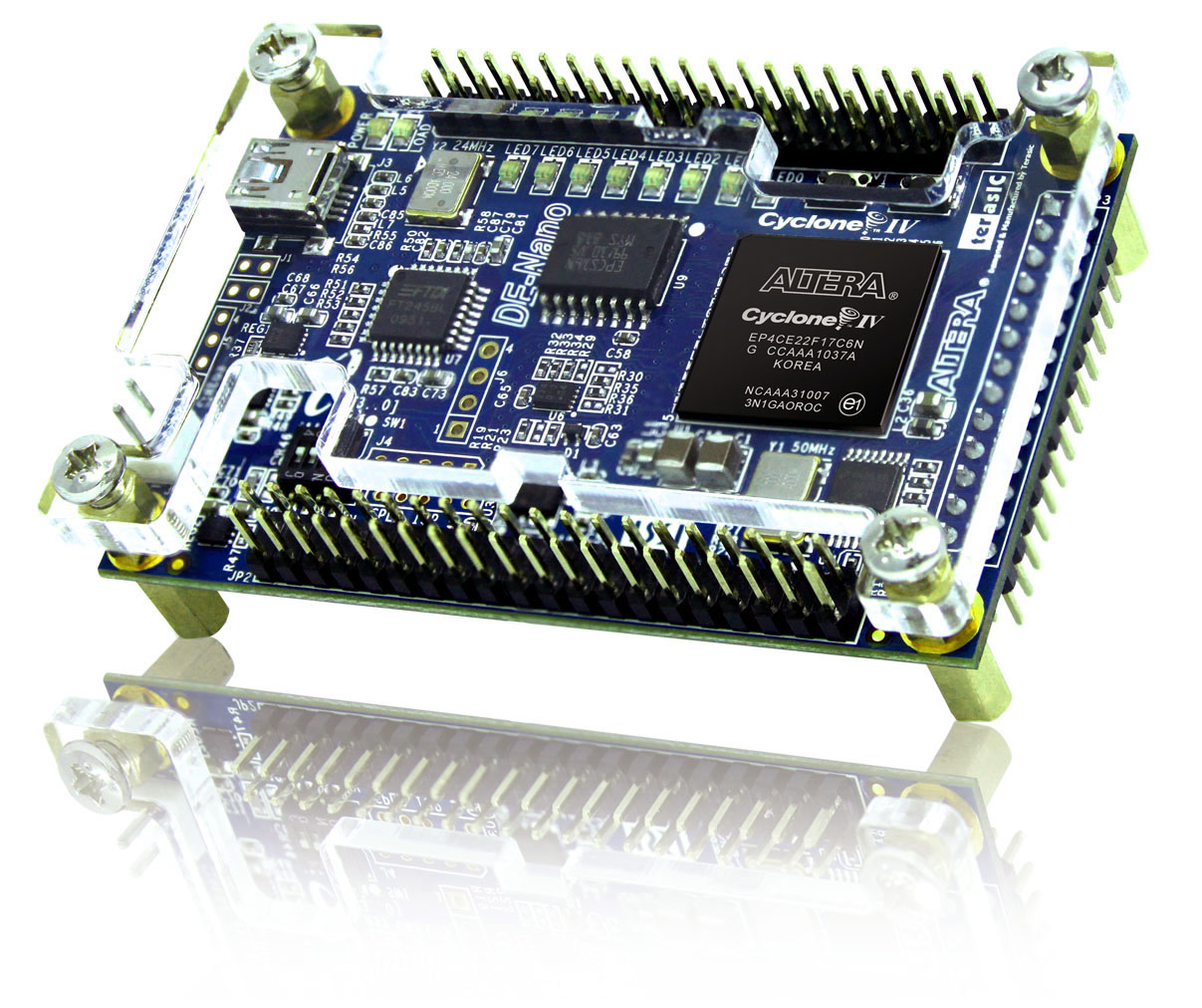
Among the many design challenges Stewart needed to overcome to replicate the AGC was converting the computer’s asynchronous RTL logic design, which was based on 3-input NOR gates, into synchronous FPGA logic. He did this by transforming the FPGA’s logic elements into clocked NOR gates. The clocking slows the FPGA’s logic to more closely replicate the timing of a 1962-era implementation based on RTL NOR gates.
Consequently, when the need arose to replace the vintage AGC’s missing rope memories and non-operational core memory with something else, Stewart had a ready solution: he had working AGC rope- and core-memory emulations all ready to go in a Cyclone IV FPGA. All that Steward needed to do was to interface the Terasic DE0-Nano board’s 3.3 V logic to the AGC’s 4 V logic with some level translators.
So that’s what he did.
For more details on the laborious, successful, and nearly miraculous AGC restoration effort, see the project’s growing YouTube playlist .
|